
SERS Applications in Soil Contamination Testing
Want to read offline? [Download PDF] Soil contamination, from heavy metals, pesticides, and polycyclic aromatic hydrocarbons (PAHs), poses serious risks to human health and ecosystems. Conventional methods such as ICP-MS, GC-MS, and HPLC remain the gold standard for confirmatory analysis, but they require sophisticated laboratory infrastructure, lengthy sample preparation, and are poorly suited to rapid
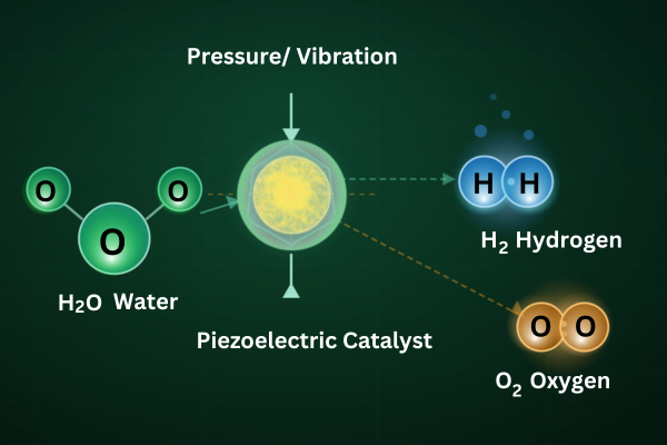
Green Energy from Water Splitting via Piezocatalysis
Want to read offline? [Download PDF] Generating green hydrogen from water splitting is pivotal to the global transition to low-carbon energy systems. Among emerging technologies, piezocatalysis, the conversion of mechanical energy directly into chemical energy via piezoelectric materials, has captured growing attention as a novel, eco-friendly approach to drive water splitting without the need for

PVD for Solid State Lithium-Ion Batteries in Space Applications
Want to read offline? [Download PDF] Spacecraft power systems operate under constraints that eliminate many conventional energy storage options. CubeSats and small satellites in low Earth orbit experience thermal excursions from −20°C to +60°C or wider, sustained exposure to ionising radiation, and hard mass and volume limits, with no option for in-orbit maintenance or electrolyte
Metal Nanoparticle Coatings on Soft Materials
Want to read offline? [Download PDF] Soil contamination, from heavy metals, pesticides, and polycyclic aromatic hydrocarbons (PAHs), poses serious risks to human health and ecosystems. Conventional methods such as ICP-MS, GC-MS, and HPLC remain the gold standard for confirmatory analysis, but they require sophisticated laboratory infrastructure, lengthy sample preparation, and are poorly suited to rapid
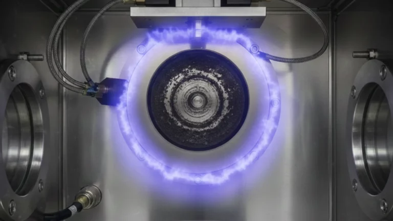
Thin Film Lithium Niobate Deposition via Magnetron Sputtering
Want to read offline? [Download PDF] Thin Film Lithium Niobate (TFLN) has become one of the most sought-after materials in modern photonics and integrated optoelectronics. With applications in telecommunications, quantum computing, photonic integrated circuits (PICs), and high-frequency electro‑optic modulators, TFLN is increasingly recognised as a cornerstone material for next‑generation optical technologies. [1],[2] Among available physical

Detecting Forever Chemicals in our waterways with SERS
Want to read offline? [Download PDF] The global water quality crisis extends across continents, with the United Kingdom facing significant contamination challenges from Per- and Polyfluoroalkyl Substances (PFAS), commonly known as forever chemicals. These synthetic compounds persist in the environment for decades, accumulating in our bodies and waterways. As regulatory agencies establish stricter drinking water
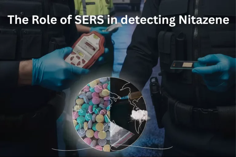
The Role of SERS in detecting Nitazene
Want to read offline? [Download PDF] The opioid crisis has entered a dangerous new phase. While fentanyl continues to dominate headlines, an even more potent class of synthetic opioids has emerged from the shadows, nitazenes. These 2-benzylbenzimidazole compounds, originally synthesized in the 1950s but abandoned due to extreme toxicity, have resurfaced on illicit drug markets
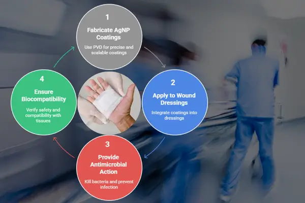
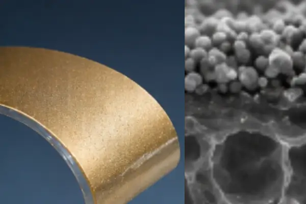
Silver nanoparticle coatings for wound dressing applications
Want to read offline? [Download PDF] In the evolving field of advanced wound care, silver nanoparticle (AgNP) coatings have become a cornerstone for developing antimicrobial dressings that are both effective and biocompatible. Among various fabrication techniques, Physical Vapor Deposition (PVD) stands out for its ability to deliver precise, reproducible, and scalable silver coatings at the
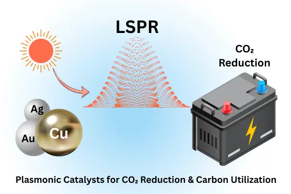
Plasmonic Catalysts for CO₂ Reduction & Carbon Utilization
Want to read offline? [Download PDF] The global push towards carbon neutrality has accelerated research into advanced catalytic systems that can convert CO₂ into valuable fuels and chemicals. Among the many emerging strategies, plasmonic catalysts for photo-thermal CO₂ reduction are gaining significant attention from researchers, students, professors, and industry experts alike. This article explores the

Why is Niobium Critical for Quantum Materials
Want to read offline? [Download PDF] Niobium (Nb) is more than a niche refractory metal, it’s a cornerstone material for next-generation electronics, superconducting devices, and quantum technologies.[1] Its unique combination of superconducting, thermal, and corrosion-resistant properties makes it essential for systems that demand extreme performance, operate at cryogenic temperatures, or function in challenging environments. In

Doped II-VI Nanocrystals for Quantum Materials
Want to read offline? [Download PDF] The field of quantum materials has seen tremendous growth, especially in quantum computing, photonics, and optoelectronics. Among the most promising materials are doped II-VI nanocrystals, which possess unique electronic and optical properties that are highly sought after for next-generation technologies. These materials are engineered at the atomic scale to
Hybrid MBE Source for Advanced Battery Electrode Deposition
Want to read offline? [Download PDF] As the demand for advanced energy storage systems continues to soar, researchers and engineers are increasingly turning to cutting-edge deposition technologies to optimize battery performance. One such innovation is the Hybrid Molecular Beam Epitaxy (MBE) Source for advanced battery electrode deposition. This hybrid approach is a game-changer for the