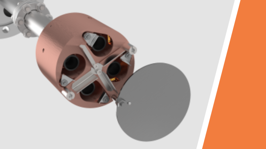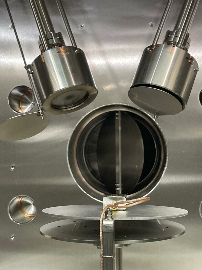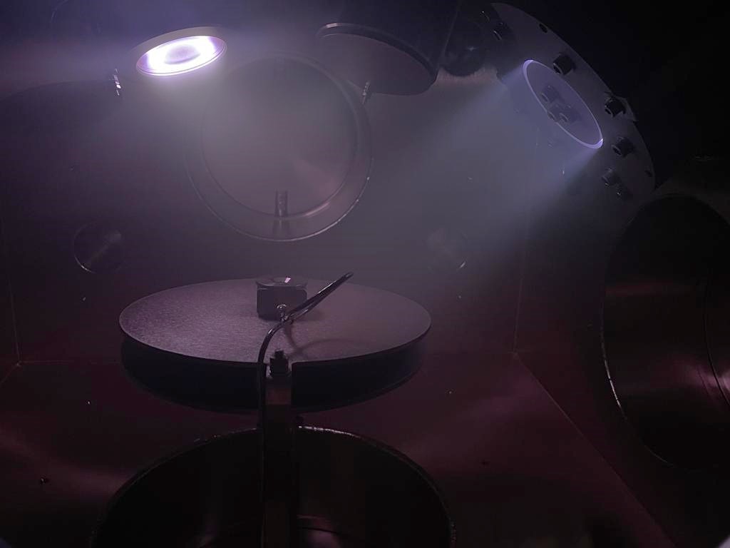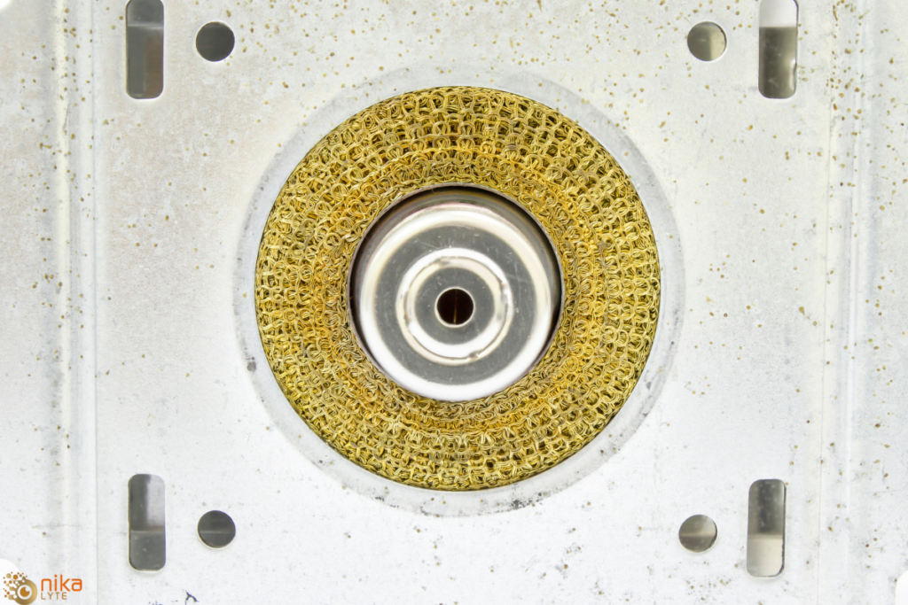
How do magnetrons work in deposition processes?
Imagine the precision required to coat a semiconductor wafer with layers just a few atoms thick or to apply flawless, glare-resistant films to camera lenses. Achieving such feats relies on the magnetron—a marvel of engineering at the core of many deposition processes. By generating controlled plasma within a magnetic field, magnetrons enable the precise sputtering […]