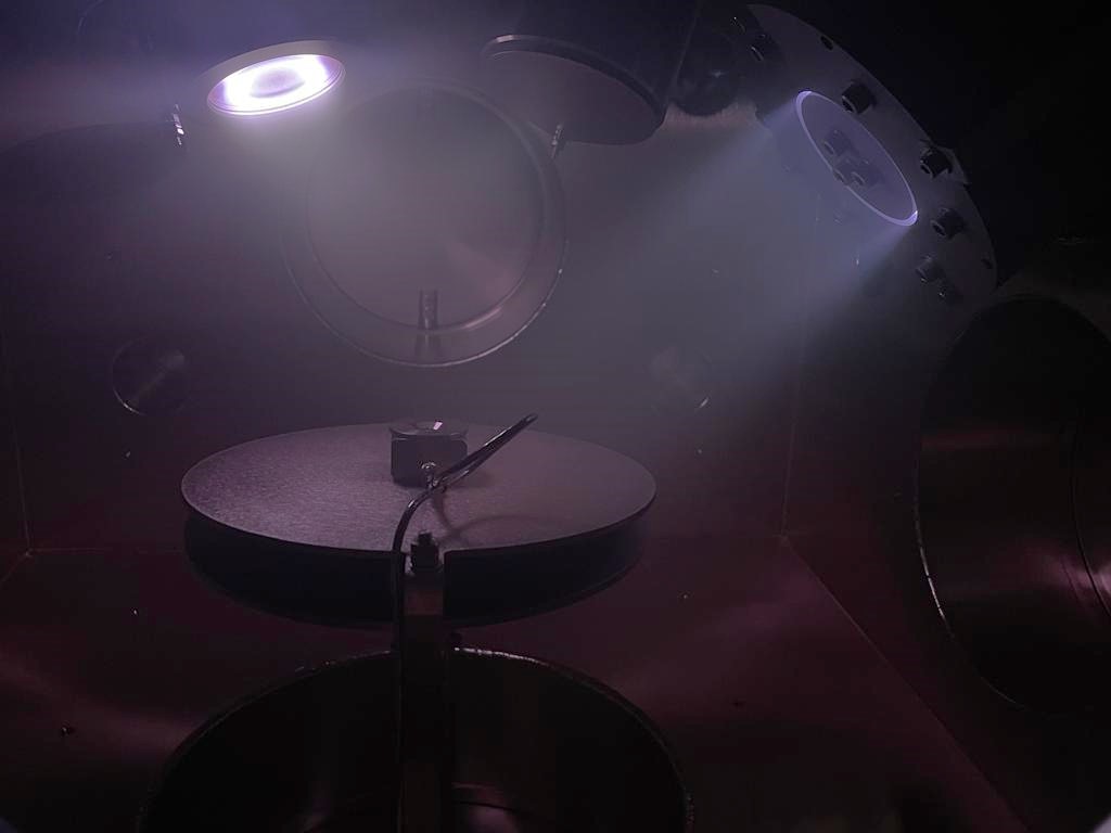
At Nikalyte we are asked quite often, “What exactly is Physical Vapour Deposition?”. Our entire business is centred around this technology and so we thought it useful to explain it in simple detail. Physical Vapour (Vapor) Deposition or PVD for short, is a form of thin film coating. There are many other methods of thin film coating, including electroplating [1], spin coating and spray coating. PVD forms the hardest and most adherent coatings available by any technique. So much so that PVD is used to coat drill bits for the oil and gas industry to increase the lifetime of drill bits. PVD is also used in other markets such as semiconductors, photovoltaics, architectural, decorative and food packaging. Generally, in PVD a solid material is vaporized, the vapor is transported through a vacuum and then condenses onto a surface.
Magnetron Sputtering.
At Nikalyte we specialise in a specific type of PVD known as magnetron sputtering [2]. The metal to be evaporated is normally referred to as the ‘target’, and the product to be coated as the ‘substrate’. We choose magnetron sputtering as it allows us to add significant energy to the evaporated material resulting in dense adherent coatings. The target material is sputtered by introducing a gas at low pressure into the vacuum of the deposition chamber. A voltage is applied to the target which allows a plasma to form above the target. The plasma is shaped by magnets behind the target. Electrons and ions are generated above the target. The ions are accelerated towards the target with enough energy to remove, or sputter atoms from its surface. As the atoms are sputtered in a vacuum they are free to travel through the vacuum towards the substrate, or product.
The sputter ‘target’ is made from very pure material, usually better than 99.99% purity, and the gases used to generate the plasma is also ultra pure. The thin film coatings generated using magnetron sputtering from ultra pure source materials, are so ultra pure which is critical for controlling the properties of these coatings.
Thin Film properties
How well do they adhere to the surface? Substrate materials and their preparation are critical to the quality of the resulting coating and will be the subject of future blogs. Briefly, the substrate is chemically cleaned before it is introduced to the vacuum chamber. It can then be heated to outgas and remove unwanted surface contamination. Finally, a glow discharge process is used to atomically clean the surface, essentially a sputtering process in itself. The surface is then ready to be coated.
Another method for controlling the thin film properties, including the adherence, is to heat the substrate during the sputtering process. The substrate will heat naturally while exposed to the plasma but it is also common practise to place the substrate on a heated sample holder. Through controlled heating of the substrate the stoichiometry, elemental makeup, of the film can be precisely controlled.
The thickness of the PVD coatings is very important for controlling the properties of the coatings. Optical coatings, for example antireflection coatings, require precise thickness of layers to interact with specific wavelength of lights. A quartz crystal microbalance is most commonly used to measure the thin film thickness in situ, as the film is deposited. A quartz crystal microbalance is placed in the chamber next to the substrate and monitors the change in vibrational frequency of a quartz crystal as the sputter material coating. Reflectivity and ellipsometry can also be used to measure the thin film coating thickness, in situ.
Reactive Sputtering
Another critical part of the PVD process is the power supply used to generate the sputter plasma. If the target material is a pure metal, or alloy then a simple DC power supply can be used. If a more complex material is to be deposited such as a metal oxide (known as reactive sputtering) then a pulsed DC power supply is used. Reactive sputtering involves the introduction of a reactive gas, such as oxygen or nitrogen in addition to the inert gas. The role of the reactive gas is to undergo chemical reaction with the sputtered metal atoms to form a compound material. This material is then deposited onto the substrate. Reactive sputtering has become an important process for depositing dielectrics, transistors and semiconductors.
It is also possible to evaporate insulating materials such a silica by using a radio frequency (RF) power supply. RF sputtering using an alternating current power source to energise the gas atoms. DC sputtering can cause a build up of charge on an insulating target. RF sputtering by contract avoids this problem by reducing the build up of ions by reversing the direction of the voltage. By controlling and optimising the deposition conditions extremely hard and adherent coatings can be deposited. Such coatings can improve the appearance of a product as well as increasing the durability, scratch resistance and decreasing coefficients of friction. PVD coated products can be found in everyday use, even on the inside of your packet of potato chips [3]!
Find out more about our flexible PVD chambers, NEXUS and NL-FLEX or contact us to speak to our technical team.
References:

